- 您现在的位置:买卖IC网 > Sheet目录3873 > PIC18F13K50-I/P (Microchip Technology)IC PIC MCU FLASH 4KX16 20-PDIP
dsPIC30F1010/202X
DS70178C-page 186
Preliminary
2006 Microchip Technology Inc.
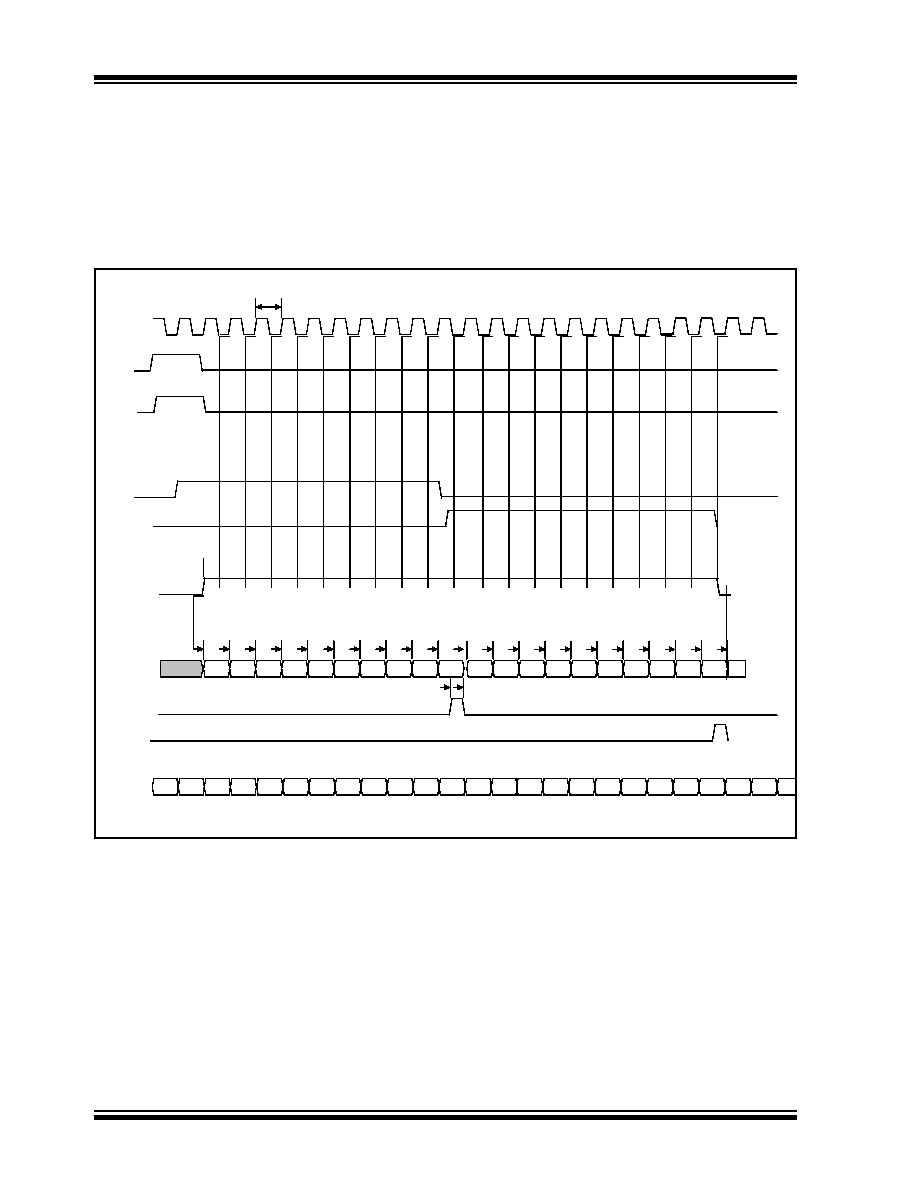
16.17 A/D Sample and Convert Timing
The sample and hold circuits assigned to the input pins
have their own timing logic that is triggered when an
external sample and convert request (from PWM or
TMR) is made. The sample and hold circuits have a
fixed two clock data sample period. When the sample
has been acquired, then the ADC control logic is noti-
fied of a pending request, then the conversion is
performed as the conversion resources become
available.
The ADC module always converts pairs of analog input
channels, so a typical conversion process requires 24
clock cycles.
FIGURE 16-3:
DETAILED CONVERSION SEQUENCE TIMINGS, SEQSAMP = 0, NOT BUSY
10th
9th
8th
7th
6th
5th
4th
3rd
2nd 1st
TAD
adc_clk
sample_even
convert_en
capture_first_data
10th
9th
8th
7th
6th
5th
4th
3rd
2nd 1st
4
5
6
7
8
9
10
11
12
13
14
15
16
17
18
19
20
21
0
1
2
0
1
2
3
connect_second
connect_first
state counter
capture_second_data
sample_odd
发布紧急采购,3分钟左右您将得到回复。
相关PDF资料
PIC16CR76T-I/SO
IC PIC MCU 8KX14 28SOIC
PIC18LF24K22-I/MV
IC PIC MCU 16KB FLASH 28UQFN
PIC18LF24K22-I/ML
IC PIC MCU 16KB FLASH 28QFN
PIC16CR76T-I/ML
IC PIC MCU 8KX14 28QFN
PIC16F627-04/P
IC MCU FLASH 1KX14 COMP 18DIP
PIC18F45J10-I/ML
IC PIC MCU FLASH 16KX16 44QFN
PIC18F24K22-I/ML
IC PIC MCU 16KB FLASH 28QFN
PIC16CR76-I/SS
IC PIC MCU 8KX14 28SSOP
相关代理商/技术参数
PIC18F13K50-I/P
制造商:Microchip Technology Inc 功能描述:20 Pin 8 KB Flash 512 RAM 15 I/O 10
PIC18F13K50-I/SO
功能描述:8位微控制器 -MCU 8KB Flash 512 RAM 15 I/O 10-B ADC USB 2.0 RoHS:否 制造商:Silicon Labs 核心:8051 处理器系列:C8051F39x 数据总线宽度:8 bit 最大时钟频率:50 MHz 程序存储器大小:16 KB 数据 RAM 大小:1 KB 片上 ADC:Yes 工作电源电压:1.8 V to 3.6 V 工作温度范围:- 40 C to + 105 C 封装 / 箱体:QFN-20 安装风格:SMD/SMT
PIC18F13K50-I/SO
制造商:Microchip Technology Inc 功能描述:20 Pin 8 KB Flash 512 RAM 15 I/O 10
PIC18F13K50-I/SS
功能描述:8位微控制器 -MCU 8KB Flash 512 RAM 15 I/O 10-B ADC USB 2.0 RoHS:否 制造商:Silicon Labs 核心:8051 处理器系列:C8051F39x 数据总线宽度:8 bit 最大时钟频率:50 MHz 程序存储器大小:16 KB 数据 RAM 大小:1 KB 片上 ADC:Yes 工作电源电压:1.8 V to 3.6 V 工作温度范围:- 40 C to + 105 C 封装 / 箱体:QFN-20 安装风格:SMD/SMT
PIC18F13K50-I/SS
制造商:Microchip Technology Inc 功能描述:8-Bit Microcontroller IC
PIC18F13K50T-I/SO
功能描述:8位微控制器 -MCU 8KB Flash 512 RAM 15 I/O 10-B ADC USB 2.0 RoHS:否 制造商:Silicon Labs 核心:8051 处理器系列:C8051F39x 数据总线宽度:8 bit 最大时钟频率:50 MHz 程序存储器大小:16 KB 数据 RAM 大小:1 KB 片上 ADC:Yes 工作电源电压:1.8 V to 3.6 V 工作温度范围:- 40 C to + 105 C 封装 / 箱体:QFN-20 安装风格:SMD/SMT
PIC18F13K50T-I/SS
功能描述:8位微控制器 -MCU 8KB Flash 512 RAM 15 I/O 10-B ADC USB 2.0 RoHS:否 制造商:Silicon Labs 核心:8051 处理器系列:C8051F39x 数据总线宽度:8 bit 最大时钟频率:50 MHz 程序存储器大小:16 KB 数据 RAM 大小:1 KB 片上 ADC:Yes 工作电源电压:1.8 V to 3.6 V 工作温度范围:- 40 C to + 105 C 封装 / 箱体:QFN-20 安装风格:SMD/SMT
PIC18F14K22-E/ML
功能描述:8位微控制器 -MCU 16KBFlash 512byteRAM 256bytesEEPROM
RoHS:否 制造商:Silicon Labs 核心:8051 处理器系列:C8051F39x 数据总线宽度:8 bit 最大时钟频率:50 MHz 程序存储器大小:16 KB 数据 RAM 大小:1 KB 片上 ADC:Yes 工作电源电压:1.8 V to 3.6 V 工作温度范围:- 40 C to + 105 C 封装 / 箱体:QFN-20 安装风格:SMD/SMT